DFM and DFT Checklist for PCB Handoff
Direct answer. Before a board is released, check it against the chosen fabricator’s and assembler’s capabilities (DFM), make sure every important net can be measured and programmed (DFT), and send one consistent, versioned file set. Confirm limits with the actual suppliers rather than generic numbers. Most first-build delays come from questions the files did not answer.
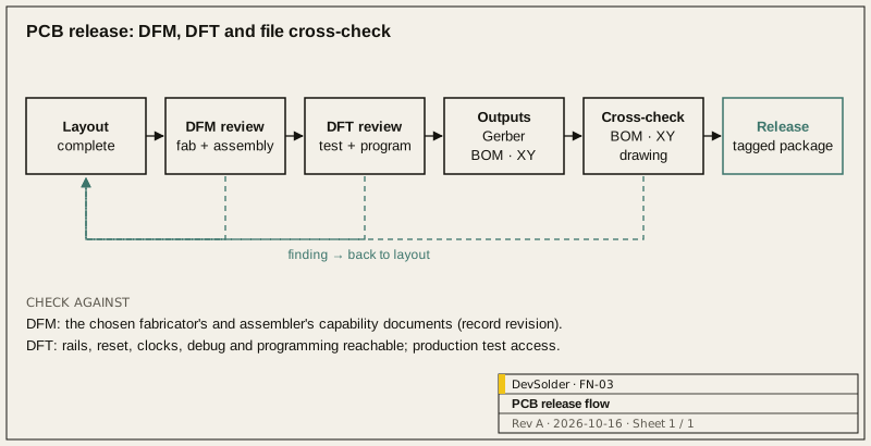
1.0 What DFM and DFT mean here
Design for manufacturing (DFM) asks whether the board can be fabricated and assembled reliably by the suppliers you intend to use. Design for test (DFT) asks whether you can find out, quickly and on every unit, that it was built correctly. Both reviews happen before release, while changes are still a layout edit and not a respin.
We do not quote generic minimum trace widths or drill sizes in this note. Those limits differ between fabricators and between their standard and advanced processes, and they change. The checklist below says what to check; the numbers come from the capability documents of the supplier you are using, and we record which document and revision we checked against.
2.0 Fabrication checks
| Item | What to confirm |
|---|---|
| Stack-up | Layer count, materials, copper weights and dielectric thicknesses agreed with the fabricator; controlled-impedance targets listed with the traces they apply to |
| Minimum features | Trace and space, annular ring, drill and via sizes within the fabricator’s standard process unless you have chosen to pay for advanced |
| Via treatment | Tented, plugged or filled vias specified, especially vias in pads |
| Copper balance | Large unbalanced copper areas reviewed for warping risk |
| Board outline and slots | Outline, cutouts, slots and plated edges on a dedicated mechanical layer, dimensioned |
| Panelisation | Who panelises; rails, fiducials, tooling holes and depaneling method (V-score or tab routing) agreed; clearance from components to the break line |
| Finish | Surface finish chosen for the parts in use, for example fine-pitch or leadless packages |
| Markings | Revision, board name and date code on silkscreen or copper; silkscreen clear of pads |
3.0 Assembly checks
| Item | What to confirm |
|---|---|
| Footprints | Each footprint checked against the manufacturer’s recommended land pattern for the exact package variant in the BOM |
| Pin 1 and polarity | Marked on silkscreen and in the assembly drawing for every polarised part |
| Fiducials | Global fiducials on the board or panel; local fiducials near fine-pitch parts if the assembler asks for them |
| Spacing | Clearance around tall parts, connectors and parts needing rework access |
| Thermal pads | Paste aperture pattern on exposed pads; via treatment under them |
| Double-sided placement | Heavy parts on the second side checked with the assembler |
| Moisture-sensitive parts | MSL from each datasheet recorded (classification per J-STD-020) so the assembler can apply J-STD-033 handling: dry-pack, floor-life tracking and bake-out |
| Through-hole parts | Soldering method (wave, selective, hand) agreed, which affects keep-outs |
| Do-not-fit parts | Clearly marked in the BOM and the assembly drawing, and consistent between them |
4.0 Test access
At bring-up you need to measure things. In production someone needs to program and test each board, often without a skilled engineer at the bench. Plan for both.
4.1 Bring-up access
- Test points on every power rail, on reset and on key clocks.
- Zero-ohm links or jumpers that let you isolate rails or subsystems during first power-on.
- The debug and programming interface on a connector or pad set that remains reachable when the board is in its enclosure, or a documented procedure if it is not.
- UART or other log output brought to a test point, even if the product does not use it.
4.2 Production test access
- Test points sized and spaced for the fixture approach you expect: bed-of-nails, pogo-pin fixture or manual probing. Confirm pad size and pitch with whoever builds the fixture.
- Test points on one side where possible.
- Programming through the fixture, so firmware loading and test run in one step.
- A self-test mode in firmware that reports results over the programming or log interface.
- Boundary scan (JTAG) chains documented where the parts support it, for boards with dense BGA nets that probes cannot reach.
4.3 Test coverage table
Write a short table listing each subsystem, how it is tested (electrical measurement, firmware self-test, functional test, visual inspection), and where. The gaps in the “how” column are the untested subsystems.
5.0 The handoff file set
| File | Purpose | Check |
|---|---|---|
| Fabrication data (Gerber X2 or ODB++ or IPC-2581) | Board fabrication | Generated from the released revision; layer list matches stack-up |
| Drill files and drill map | Holes, plated and non-plated | Units and format stated; matches fabrication data |
| Fabrication drawing | Stack-up, impedance, finish, tolerances, notes | Revision matches files |
| Pick-and-place (centroid) file | Placement | Rotation convention stated; spot-checked against assembly drawing |
| BOM | Parts, quantities, reference designators, manufacturer part numbers, approved alternates | Every placed reference has a line; DNF parts marked |
| Assembly drawing | Placement, polarity, special instructions | Matches BOM and centroid |
| Schematic PDF | Debug and review | Same revision |
| Test specification | What to test and how | Matches test points on the board |
| Release notes | What changed since the previous revision | Lists open issues |
The most frequent handoff error we look for is inconsistency: a BOM from one revision, a centroid file from another, a part marked DNF in one place and fitted in another. A scripted cross-check between BOM, centroid and design data catches most of it.
Everything goes into a versioned archive with the revision in the file name, and the same revision is tagged in the design repository.
6.0 Who does what
Where DevSolder prepares a Build-Ready Hardware Package, these checks and the file set are part of the delivery. You can then source and build yourself, or ask us to arrange sourcing and assembly; the files are the same either way. Your contract manufacturer will run its own DFM review as well; get its comments before the order is placed.
See the Hardware Design Package page for the deliverables, Assembly, Bring-up and Test for the bring-up side, and Sourcing and Manufacturing for supplier work. To ask for a review of a board before release, use the Discuss a Project form.
References
- Ucamco, The Gerber Format: https://www.ucamco.com/en/gerber
- IPC-2581 Consortium: https://www.ipc2581.com/
- IPC/JEDEC J-STD-020F, Moisture/Reflow Sensitivity Classification: https://www.jedec.org/standards-documents/docs/j-std-020e
- IPC/JEDEC J-STD-033D, Handling, Packing, Shipping and Use of Moisture/Reflow Sensitive SMDs: https://www.jedec.org/standards-documents/docs/j-std-033c
Frequently asked questions
Our assembler says they do a DFM check. Do we still need one?
Their check tells you whether they can build it. It usually does not tell you whether the board can be tested, debugged or sourced over the product's life. Doing your own review first means their comments are about their process, and you are not finding basic errors through their queue.
Should we use Gerber or IPC-2581?
Use the format your fabricator handles best and ask them. Gerber X2 with drill files and a fabrication drawing is widely accepted. IPC-2581 and ODB++ carry more of the design intent in one package, which reduces the chance of mismatched files.
How many test points are enough?
Enough to measure every rail, reset and key clock at bring-up, and to program and run the production test without manual probing. A coverage table per subsystem makes gaps visible, which is more useful than a target count.
Can you review a board someone else designed?
A review of an existing design works the same way: we check it against the target suppliers' capabilities, the test plan and the file set, and return a written list of findings ranked by impact on the build.